Projects Archive
MOEMS Display Technology - Transmissive Electrostatic Micro-Optic Switches
Team Members
Kerwin Wang, Karl F. Böhringer, Mike Sinclair (Microsoft Research), Gary Starkweather (Microsoft Research)
Summary
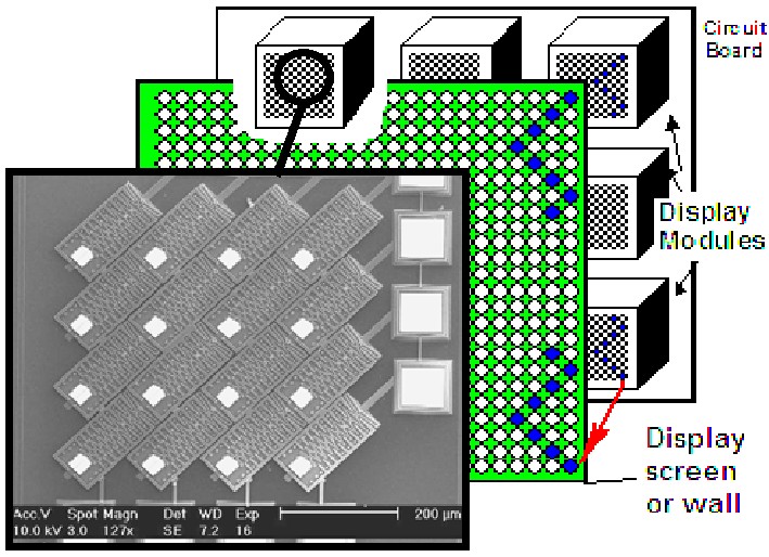
This work presents likely the world's smallest electrostatic visible light highly space-efficient transmissive micro-optical switches (TMOS) for an integrated MEMS optical display system. Each TMOS represents one pixel with 150µm x 150µm spacing in a display module. It is demonstrated that a zigzag electrostatic actuator of 47µm x 160µm size can achieve a maximum static lateral displacement of 10µm at 38V. Depending on the zigzag actuator design, these devices have a mechanical resonance frequency of up to 18.6kHz.
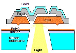
The TMOS consists of an electrostatic "zigzag" actuator pair, overlapping shutters and a miniaturized optical tunnel. The dimensions of these three components are mainly depending on the optical configuration. A microlens array can focus light into the aperture to minimize the optical loss. A second microlens array placed behind the TMOS array will image the light onto a display screen area or a projector lens. Assuming the light presented to the first microlens array has a nearly planar wave front, then each microlens focuses its portion of the light into the aperture adjacent to the shutter (Figure 2). The shutter can modulate the light by controlling its opening. A small spot size only needs a small shutter and movement to fully turn the light on and off. It also implies low driving voltage, low power consumption, and higher frequency operations. The minimal spot size and the profile of the optical tunnel are mainly constrained by the depth of focus, diffraction spot size and the numerical aperture of the selected microlens system.
 |
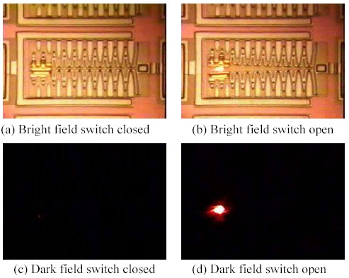
Figure 3: The shutter can successfully switch the light on and off. Optical test results show that this TMOS can achieve near-ideal contrast ratios. |
Selected Publications
-
Kerwin Wang, Karl F. Böhringer, Mike Sinclair, Gary Starkweather, "Highly Space-efficient Electrostatic Zigzag Actuator for Transmissive Micro-Optic Switches." The 12th International Conference on Solid-State Sensors and Actuators (Transducers'03), Boston, MA, June 6-12, 2003. Paper. Poster.
A complete list of our publications (many of them available online) can be found here.
Acknowledgements
-
Supported by Microsoft Research


